
Architecture Diagram
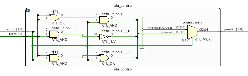
ALU Control
參考簡報第 34 頁的圖,然後加了一個 MUX 來擴充 lui、ori。
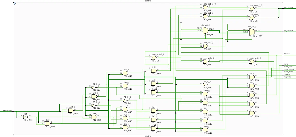
Main Control
參考簡報第 32 頁的圖,使用 PLA (Programmable Logic Array) 來設計,這樣也方便擴充 j 指令。
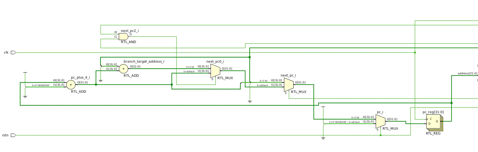
Single Cycle CPU
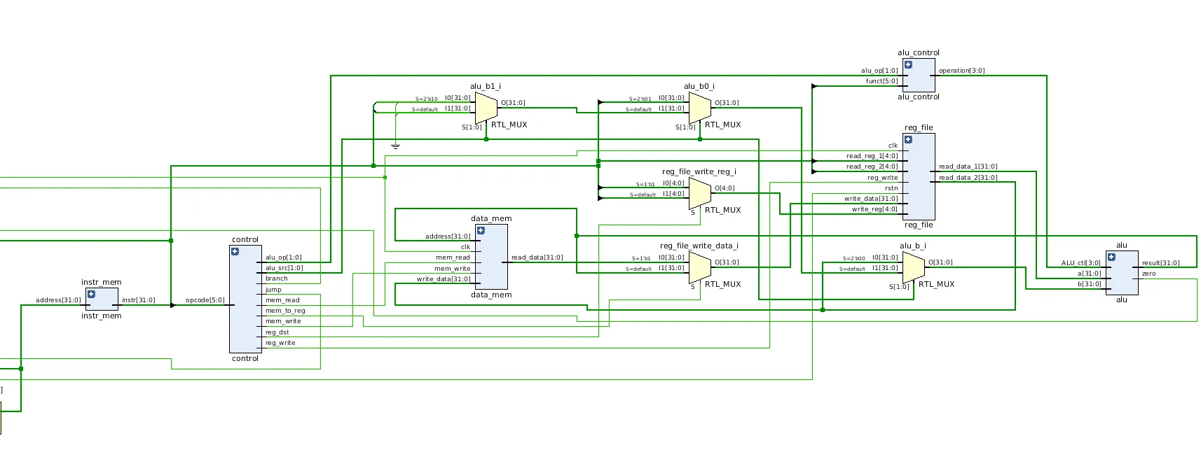
Write Register MUX:由 RegDst 訊號控制。
- 當
RegDst = 1時選擇rd欄位(用於 R-type) - 當
RegDst = 0時選擇rt欄位(用於 I-type)。
ALUSrc MUX:修改課本擴充成 2-bit 的 alu_src。詳細說明在 Problems Encountered and Solution。
MemtoReg MUX:由 MemtoReg 訊號控制。
- 當
MemtoReg = 1時選擇 Data Memory 的讀出資料。 - 當
MemtoReg = 0時選擇 ALU 運算結果。
Next PC MUXes: 由 Main Control 的 Branch 與 Jump 訊號,配合 ALU 輸出的 Zero 訊號共同控制。- 如果 Branch & Zero = 1 則選擇 branch_target_address
- 如果
Jump = 1則選擇jump_target_address - 以上皆不滿足則選擇
pc + 4
Experimental Result
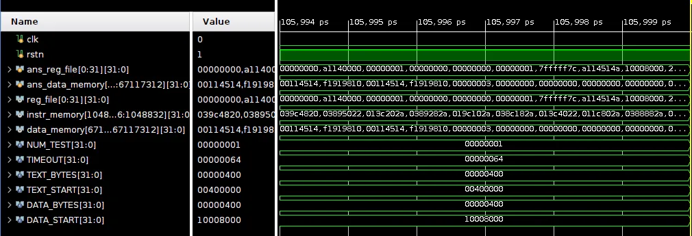
Answer the Following Questions
When does write to register/memory happen during the clock cycle? How about read?
write to register/memory 是正緣觸發的 sequential logic,固定發生在 clock signal 的 positive edge。
read from register file/memory 是組合電路,只要輸入訊號有變動就馬上會立刻把值輸出到排線上(delay 來源是 logic gates)。
Translate the “branch” pseudo instructions (blt, bgt, ble, bge) in the Green Card into real instructions. Only at register can be modified, and other common registers should not be modified.
# equivalent to "blt $s1 $s2 offset"
slt $at $s1 $s2
bne $at $zero offset

# equivalent to "bgt $s1 $s2 offset"
slt $at $s2 $s1
bne $at $zero offset

# equivalent to "ble $s1 $s2 offset"
slt $at $s2 $s1
beq $at $zero offset

# equivalent to "bge $s1 $s2 offset"
slt $at $s1 $s2
beq $at $zero $offset
Give a single beq assembly instruction that causes infinite loop. (consider that there’s no
delay slot)
beq $zero $zero -1The j instruction can only jump to instructions within the “block” defined by “(PC+4)
[31:28]”. Design a method to allow j to jump to the next block (block number + 1) using another j.
假設現在的 block number 是 5,想法是先跳到當前 block 的最後一個位置,然後在最後一個位置 j 時 PC+4 就會在下一個 block,順利吃到下一個 block number。
0x5???????  j 11111111111111111111111111

...

0x5FFFFFFC  j 00000000000000000000000011      BLOCK 5
-----------------------------------------------------
0x60000000                                    BLOCK 6
0x60000004
...
0x6000000C  # (Finally Goes Here)
Why a Single-Cycle Implementation Is Not Used Today?
所有指令都要在一個週期內完成的話,瓶頸會卡在某個最慢的指令(通常就是 lw 因為 lw 要經過 IF > ID > EX > MEM > WB 這 5 個 stages),導致時脈提升會有上限。另外也沒辦法將指令平行化處理(pipeline),會有硬體資源 idle。
Problems Encountered and Solution
這份 lab 的目標是做出一個最小可動的 CPU,所以我選擇了不靠 AI 自己動手寫,這樣才能真正學到東西,而且助教寫的提示超級詳細,跟課本的圖對照著做就能順利做出來。
然後首先是擴充 j 指令,想了一段時間後,最後發現現有的 control signals 沒辦法優雅地相容 jump 操作(jump 的定址方式跟 branch 是異質的),所以就在 control.v 的 output 加上了一個 jump 訊號,並且開一條新的 sub-datapath 算指令為 jump 時的目標 PC。
lui ori 比較麻煩,花了一點時間想該怎麼擴充現有的設計。後來的解決方案是:
- 不需要開新的 control signals,都可以用現有的訊號控制。
alu_op[1:0]剛好還有11這個值沒用到,所以就直接拿來配給lui、ori這兩個語意上相近的操作。- ALU 的
alu_b緊接在前的 MUX 從 2 個通道改成 4 個通道,分別是:00: $rt01: sign-extended immediate10: zero-extended immediate (ori)11: lui-extended immediate (lui,就是把 16 bits immediate 丟到高位)與之對應的alu_src也要擴充成alu_src[1:0]。但是alu_control.v那邊我就偷懶了,懶得畫卡諾圖重新優化電路,所以就直接硬插一個三元運算。
然後最後在 Vivado 跑 simulation 時,不小心跑出 Time Limit Exceeded。盯著 code 盯了很久才發現有兩個地方沒改到:
single_cycle_cpu.v第 90 行那邊的alu_src排線忘記修改成 2-bit output。- 第 121 行那邊的
jump_target_address,裡面的instr_mem_instr打錯打成instr_mem_address(code completion 自動補上但我沒檢查到)。 上面兩個 bugs 都會讓 PC 跳出界,然後就一直不斷執行nop(讀到的指令永遠都是0x00000000)。
Feedback
助教的提示都寫得很詳細!